SEC 02 / PINOUTS
40-pin map & alternate functions
The complete LGA-56 pin assignment: default function, alternate mux, drive strength, and power domain — copyable into your schematic.
REV 2.4PKG LGA-56
2.1
Reading the map
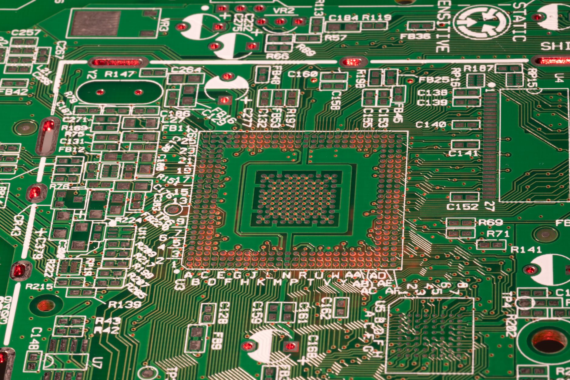
Pin 1 is marked by the corner dot on the top-side silkscreen. Numbering runs counter-clockwise. Every GPIO can be remapped through the pin-mux; the alternate column lists the highest-priority function.
PWRSupply / ground
GPIOGeneral purpose I/O
ANAAnalog-capable
STRAPBoot-strap, do not load
2.2
Full pin table
| Pin | Name | Default | Alternate | Role |
|---|---|---|---|---|
| 1 | VDD | 3.3 V supply | — | PWR |
| 2 | GPIO0 | Boot select | UART0_TX | STRAP |
| 3 | GPIO1 | I/O | UART0_RX | GPIO |
| 4 | GPIO2 | I/O | SPI0_SCK | GPIO |
| 5 | GPIO3 | I/O | SPI0_MOSI | GPIO |
| 9 | GPIO7 | Analog in | ADC0_CH2 | ANA |
| 14 | GPIO12 | I/O | I2C0_SDA | GPIO |
| 15 | GPIO13 | I/O | I2C0_SCL | GPIO |
| 28 | GPIO26 | I/O | PWM4 | GPIO |
| 36 | GPIO34 | Input only | ADC1_CH5 | STRAP |
| 56 | GND | Ground | — | PWR |
2.3
Remapping the mux
Any peripheral signal can be routed to any GPIO through the pin-mux matrix. Write the function index to the pin's control register, then enable the pad. The snippet routes UART1 onto GPIO20/21.
NOTE
Strap pins latch their function at reset. Never remap GPIO0 or GPIO34 before the boot sequence completes.
pinmux.c
// route UART1 to GPIO20 (TX), GPIO21 (RX)
mux_select(GPIO20, FN_UART1_TX);
mux_select(GPIO21, FN_UART1_RX);
pad_enable(GPIO20 | GPIO21);
uart_init(UART1, 115200);